Founded in the early 1990’s, NVIDIA is known for its processor units used in AI, data science, and high-performance computing, and in computers, gaming consoles, and autonomous vehicles worldwide.
As expected, a global leader such as this has a robust R&D infrastructure and requires extensive onsite testing and failure analysis for multiple product lines. De-risking designs and finding failure points before production begins is critical to the success of any project.
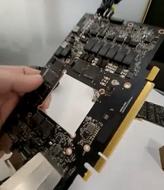
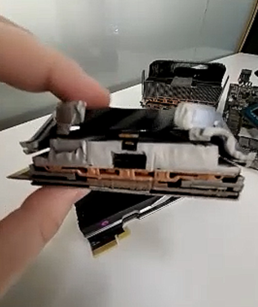
Jonathon, an engineer with the company, explained their failure analysis (FA) process. His department cuts out semiconductor material destined for the manufacturing process, including chips, components, etc. to measure failure rates and determine the quality of the raw material. The standard industry process previously was a wet saw and chemicals, which generates heat and has accuracy issues.
“[The WAZER] is a welcome asset”
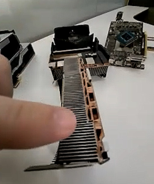
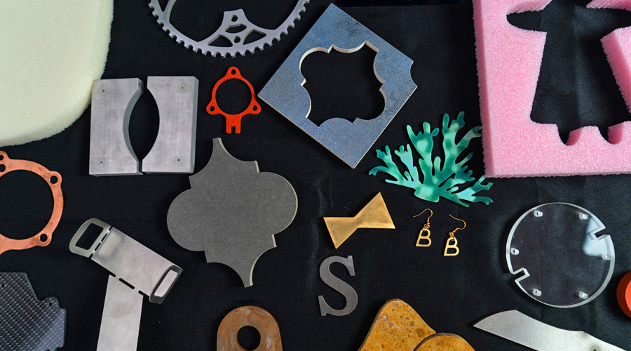
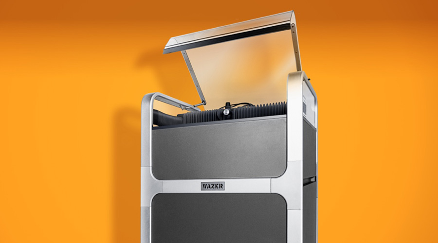
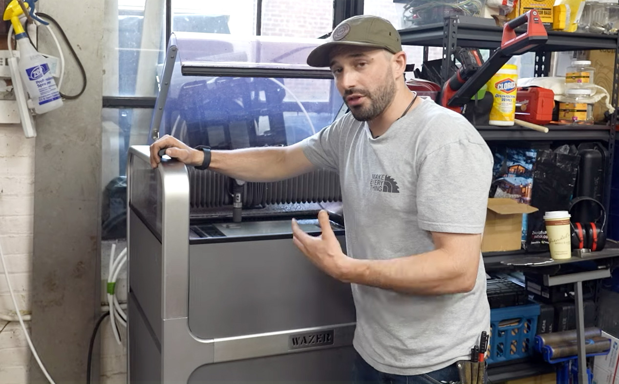
With the WAZER, there is no heat generated, no chemicals needed, and the process is much more accurate and efficient. “It’s a big selling point”, Jonathon noted. Jonathon and his team are using their WAZER for a variety of jobs multiple times per week: “We’ve been relying on it pretty heavily, it’s a welcome asset.” Jonathon emphasized they also found the low entry cost to be an asset as well, “anything under $10k for a large tech company is no problem, above that, you need more approvals.”

